- The heat flow is changed inside the chip components instead of being removed after build-up
- Phonon motion is limited through nanoscale surface patterning
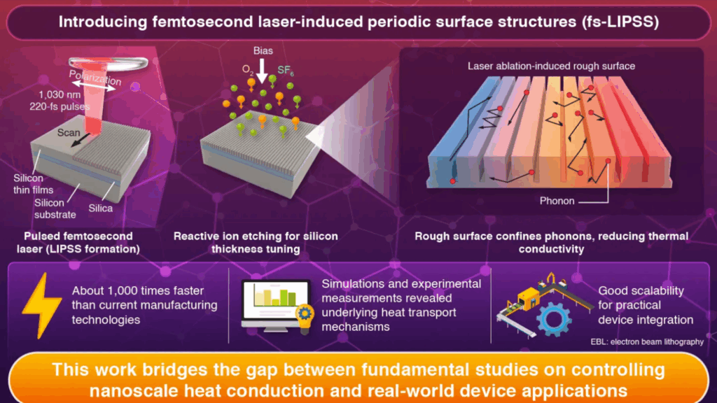
- Ultrafast lasers enable nanoscale patterning at industrially relevant speeds
Today, most electronics rely on heatsinks, fans or liquid cooling because the components inside the chips conduct heat in fixed ways.
A new method designed by Japanese researchers lets engineers control how quickly heat escapes from a material, rather than simply trying to remove heat after it’s built up.
The work describes a laser-based fabrication method that modifies how heat travels through thin silicon and silica films by directly shaping their surfaces at the nanoscale.
Change of heat transport at chip component level
The process relies on ultrafast laser pulses, each lasting a femtosecond, to remove material and create parallel grooves across the film surface.
These grooves are formed with carefully controlled spacing and depth that closely matches the average distance the phonons travel before scattering.
Because phonons are the primary carriers of heat in these components, limiting their motion predictably changes the overall thermal conductivity.
The resulting features, known as femtosecond laser-induced periodic surface structures, show high uniformity over relatively large areas.
When combined with conventional dry etching to adjust the film thickness, the patterned surfaces exhibit a marked reduction in thermal conductivity.
Thermoreflectance measurements quantified this change, providing experimental confirmation rather than inferred behavior.
Numerical simulations also showed that the reduction is mainly due to limited phonon travel distances rather than changes in chemical composition or bulk material properties.
A central claim in the study concerns manufacturing speed. The fs-LIPSS process is reported to operate at a throughput more than 1000x faster than single beam electron beam lithography while still achieving nanoscale resolution.
This difference is significant, especially for applications that require large patterned areas, such as thermal layers integrated into data center-class processors.
The process is maskless and resistless, reducing procedural complexity and conforming to standard CMOS manufacturing constraints.
The technique has also been described as capable of wafer-scale implementation without introducing additional components or lithographic steps.
Because the method avoids resists and masks, it remains compatible with established semiconductor workflows.
The researchers describe the process as scalable, semiconductor-ready and suitable for integration with existing manufacturing lines.
The nanostructures are described as mechanically robust, with reports indicating strength levels up to 1000x higher than those produced using some conventional patterning methods.
However, the available description provides limited details on direct mechanical benchmarking or comparative test methods.
The technique looks promising and is relevant to high-performance computing, quantum devices and thermal management challenges associated with dense GPU clusters that power modern AI tools.
But wider adoption will depend on reproducibility, long-term stability and cost under industrial conditions, especially at data center deployment scales.
Via Institute of Science Tokyo
Follow TechRadar on Google News and add us as a preferred source to get our expert news, reviews and opinions in your feeds. Be sure to click the Follow button!
And of course you can too follow TechRadar on TikTok for news, reviews, video unboxings, and get regular updates from us on WhatsApp also.