- Peking University Transistor could surpass Intel, TSMC and Samsung’s top silicon chips
- Full door covering increases speed and cuts energy consumption in breakthrough Chinese transist word design
- China may have just led by the US chip-tech with this silicon-free transistor innovation
Chinese researchers at Peking University have announced what looks like a breakthrough in transist word design, as if commercialized, could dramatically move the direction of microprocessor development.
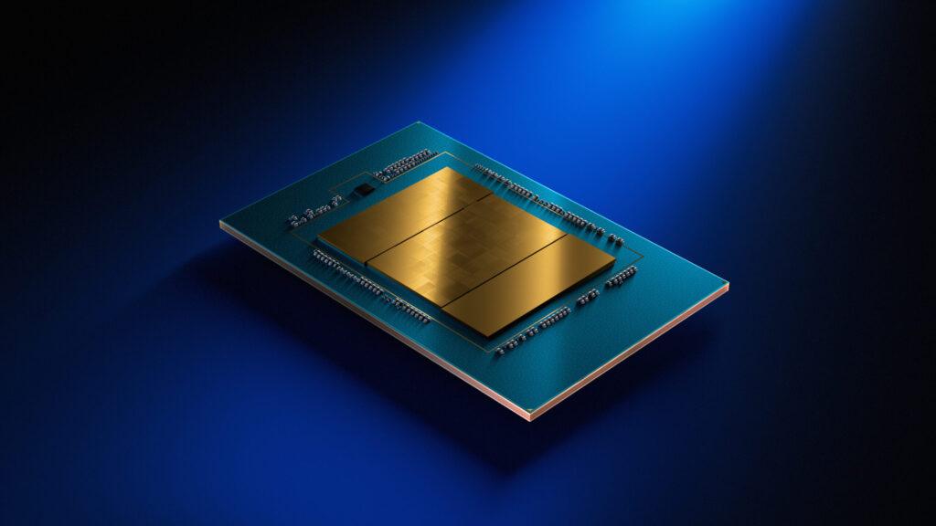
The team created a silicon-free transistor based on a two-dimensional material, Vismuth Oxyselenid.
The innovation is linked to Gate-All-Around (Gaafet) architecture, where the transistor’s gate packs all the way around the source. Traditional Finfet design, which dominates current silicon-based processors, allows only partial port coverage. This full wrapping structure improves the contact area between the gate and the channel, which improves performance by reducing energy leakage and enabling better power control.
Could this mark the end of silicon chips?
Published in Natural materialsIf the paper suggests that the new 2D Gaafet could compete or even surpass silicon transistors in both speed and energy efficiency.
The researchers claim that their 2D transistor achieves speeds 40% faster than Intel’s latest 3NM chips, while using 10% less power, performance that would place it in front of the current processors from TSMC and Samsung.
The partial port coverage in traditional design limits current control and increases energy loss. The new full gate structure addresses these problems, resulting in high-voltage gain and ultra-low power consumption. The team has already designed small logical devices using the new design.
“It’s the fastest, most effective transistor ever,” said Peking University. These claims are supported by tests performed under identical conditions with those used for leading commercial chips.
“If chip innovations based on existing materials are considered a ‘shortcut’, our development of 2D material-based transistors is akin to ‘changing courses’,” said Professor Peng Hailin, the project’s leading scientist.
Unlike the vertical structures of Finfets, the new design is similar to interwoven bridges. This architectural shift can overcome miniaturization limits that silicon technology faces, especially when the industry pushes under the 3NM threshold. It can also benefit the fastest laptops that require such compact chips.
The team developed two new bismuth-based materials: BI₂OFS as semiconductor and BI₂SEO₅ as a port dielectric.
These materials have low interface energy, reduction of defects and electron spread.
“This allows electrons to flow with almost no resistance, like water through a smooth tube,” money explained.
The performance results are supported by density function theory (DFT) calculations and validated through physical tests using a high precision factory at PKU.
The researchers claim that transistors can be manufactured using the current semiconductor infrastructure and simplify future integration.