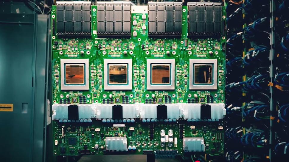
- Google’s Ironwood TPU scales for 9216 chips with record 1.77pb shared memory
- Dual Die Architecture delivers 4614 TFLOPS FP8 and 192 GB HBM3E per Chip
- Improved cooling of reliability and AI -assisted design functions enable effective inference workload in scale
Google closed Machine Learning Sessions on the recent Hot Chips 2025 event with a detailed look at its latest Tensor Processing Unit, Ironwood.
The chip, first revealed on Google Cloud Next 25 back in April 2025, is the company’s first TPU, which is primarily designed for a large -scale -infer workload rather than training and arrives as its seventh generation of TPU hardware.
Each Ironwood chip integrates two calculation disles and delivers 4,614 TFLOPS of FP8 performance -and eight stacks of HBM3E give 192 GB memory capacity per day. Chip, paired with 7.3 TB/S bandwidth.
1.77PB of Hbm
Google has built -in 1.2 Tbps of I/O ribbon width to allow a system to scale up to 9,216 chips per day. Pod without glue logic. This configuration reaches a full 42.5 exaflops of performance.
Memory capacity also scales impressive. Across a pod, Ironwood offers 1.77PB direct addressable HBM. This level sets a new record for shared memory super computers and is activated by optical circuit contacts connecting racks together.
The hardware can configure around unsuccessful nodes and restore workloads from checkpoints.
The chip integrates several functions aimed at stability and resilience. These include an on-chip root of trust, built-in self-test functions and measures to mitigate silent data corruption.
Logical repair features are included to improve production yield. A emphasis on ras or reliability, accessibility and service is visible throughout the architecture.
Cooling is handled by a cold plate solution supported by Google’s third generation of fluid cooling infrastructure.
Google claims a double improvement of performance per Watts compared to trillium. Dynamic voltage and frequency scaling further improve efficiency during different workloads.
Ironwood also incorporates AI techniques within its own design. It was used to help optimize ALU cycling and floor plan.
A fourth generation SparSecore has been added to speed up embedders and collective operations that support workloads such as recommendation engines.
Implementation is already underway on Hyperscale in Google Cloud data centers, though the TPU remains an internal platform that is not available directly to customers.
Comment on the session on Hot Chips 2025, ServethehomeRyan Smith said: ‘This was a great presentation. Google saw the need to create advanced AI calculation many generations ago. Now the company is innovating at all levels from chips, the interconnections, and to the physical infrastructure. Even when the last Hot Chips 2025 presentation had this, the audience had turned on the stage of what Google showed.