- SanDisk says that 3D -matrix memory will be an affordable replacement for dram
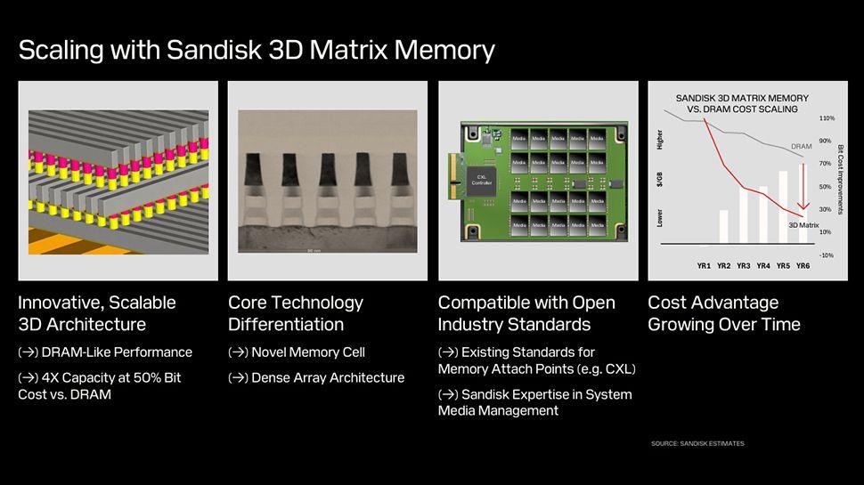
- Will provide dram-like performance to 4x capacity and half the cost
- SanDisk says it will be more affordable when the technology matures
On its recent Sandisk 2.0 Investor Day session, the flash storage giant revealed a number of new SSDs, including a 128TB data center model, while outlining its ambitious roadmap for even greater drive – EN 256TB SSD in 2026, a 512TB SSD in 2027 and a huge 1pb – Driving expected a few years later.
SanDisk is eager to reassure any investor Wobbles after his split from Western Digital, and in addition to discussing his strategy to increase returns and margins, the company also took the wrapping of its groundbreaking 3D matrix memory, a scalable memory technology that reportedly promises dram-like Performance four times the capacity and half of the cost.
SanDisk has placed 3D matrix memory as an affordable solution in response to the end of Moore’s law for drama, where scaling of stagnation, an extended computer memory gap and soaring memory costs have become major challenges. The company says its scalable memory architecture will break through the “memory wall” and solve the problem of memory capacity and bandwidth struggling to keep up with ever -increasing treatment requirements.
More cost effective
Sandisk’s 3D matrix memory was developed in collaboration with IMEC and is built on a close array architecture with a new memory cell design, while maintaining compatibility with open industrial standards, such as CXL.
The company claims that its new memory technology is becoming more and more cost -effective over time. According to a graph, SanDisk is divided, 3D matrix memory in year 6 will achieve over 50% cost savings per year. Bit compared to DRAM, with a marked steeper fall in $/GB, making it a more affordable alternative to traditional DRAM solutions.
The company’s development schedule, shown below, outlines a number of milestones, with the transition from a 150 mm WD research FAB to a 300 mm IMEC facility in 2024, marking the technique’s first important step towards large-scale production.
From 2017, the project has evolved from isolated units to passive arrays, to CMOS development vehicles. Gen1 media tests will be the next big step and these are expected to reach 32-64Gbit capabilities, although there are no details of raw performance yet.