- Researchers at IMEC have found a way to grow lasers directly on silicon
- IMECS lasers use Galliumarsenide, a material that does not naturally bind with silicon
- This breakthrough could lower costs and improve photonic chips for AI and Telekom
Silicon photonics use light to transmit data instead of relying on electrical signals, but since silicon itself cannot effectively generate light, it requires lasers as a light source.
Placing lasers on chips has traditionally been a challenge, as silicon – a material often found in sand – is not suitable for the manufacture of lasers, and the best laser materials, such as gallium arsenide (GAAS), do not work naturally with it. Existing methods require binding these materials on silicon, a process that is both expensive and wasted.
Researchers at the Belgium Research Center IMEC have come up with a solution to this problem involving growing lasers directly on silicon. This discovery can lead to more affordable and scalable photonic devices that potentially transform applications in data communication, machine learning and AI.
Short wavelengths
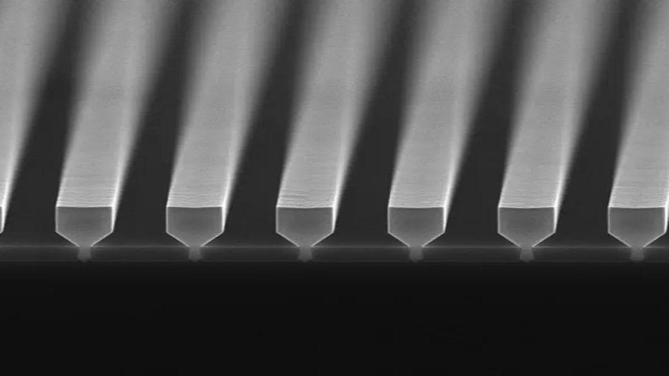
IMECS approach, detailed in a paper published in Natureis based on nano-ridge engineering, which limits defects that would otherwise impair laser performance.
They start with IEEE SPECTRUM describes it). Gallium arsenide is then deposited in these trenches, where it only comes into contact with silicon at the bottom. This location keeps the defects buried in the ditch and prevents them from spreading in the laser material above.
The lasers use Indium Galliumarsenid (Ingaas) several quantum wells such as the optical reinforcement region and are embedded in a doped PIN diode structure. They work at room temperature with electrical injection with continuous wave, achieving threshold streams as low as 5 ma and output forces of up to 1.75 MW.
“In the last years, IMEC has groundbreaking Nano-Ridge Engineering, a technique that is based on a case [selective-area growth] and art [aspect-ratio trapping] To grow with low defective III-V nano-ridges outside the trenches, ”said Bernardet Kunert, scientific director at IMEC.
“Now IMEC III-V Nano-Ridge Engineering Concept to demonstrate the first full scale of electrically pumped GAAS-based lasers on standard 300 mm silicon discs, completely within a CMOS pilot making line.”
The nanoridge -lases emit light at 1,020 nanometers, which IEEE SPECTRUM Pointed out, is a shorter wavelength than those typically used in telecommunications. IMEC’s researchers say they are actively working to expand the wavelength and improve the design to reduce defects near electrical contacts. If successful, this approach could provide a scalable and cost -effective solution to integrate lasers into silicon photonics, which paves the way for the future high -performance optical devices.