- Photonic chips with quantum lasers are finally built without redesigning the whole system
- These lasers work directly on silicon and still survive high heat for over six years
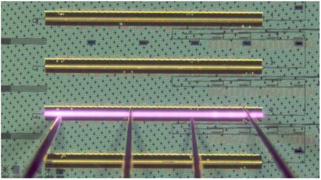
- University of California scientists filled the laser gap with polymers and spiced precision beam control on-chip
A new manufacturing method could make photonic circuits cheaper and more convenient by directly integrating the Quantum Dot (QD) lasers on silicon chips, a process that can affect how future smart home units, fitness trackers and even laptops are constructed.
The research team, led by Rosalyn Koscica at the University of California, achieved this by combining three key strategies.
They used a pocket laser configuration for direct integration, followed a two-stage growth method involving metal organic chemical steam deposits and molecular beam epitaxy and introduced a polymergap filling technique to reduce optical radiation spread.
Closing the gap with careful technique
This development relates to many years of challenges involving material incompatibility and linking inefficiency that has historically limited the benefit and scalability of integrated photonic systems.
The combined effort minimized the initial interface hole and enabled lasers to function reliably on silicon photonic chiplets.
As researchers note that the “Photonic Integrated Circuit (PIC) applications call for on -chip light sources with a small device’s footprint to allow closer component integration.”
The new approach enables stable lasing with a single state at the O-band frequency, which is suitable for data communication in data centers and cloud storage systems.
By integrating the lasers directly with ring resonators made of silicon or using distributed bragg reflectors from silicon nitride, the team has also treated problems related to adaptation and optical feedback.
One of the more surprising findings from the research is how well the lasers are doing under heat.
“Our integrated QD lasers demonstrated a high temperature lasing up to 105 ° C and a life of 6.2 years while working at a temperature of 35 ° C,” says Ms. Koscica.
These benefit metrics suggest a level of thermal stability that was previously difficult to achieve with monolithic integrated design.
This thermal resilience opens the door to more durable uses in the real world environments where temperature fluctuations can limit the reliability of photonic components.
It can also reduce the need for active cooling, which has traditionally added costs and complexity to previous design.
In addition to performance, the integration method seems suitable for large -scale production.
Because the technique can be performed in standard semiconductor foundries and does not require major changes in the underlying chip architecture, it promises the vider adoption.
The researchers claim that the method is “cost -effective” and “can work for a variety of photonic integrated chip design without needing extensive or complex changes.”
That said, the procedure is likely to face control of consistency across large slices and compatibility with commercial photonic systems.
Success in controlled laboratory environments also does not guarantee trouble -free implementation in mass making settings.
The combination of a compact laser design, compatibility with conventional processes and integration of O-band functionality makes this development remarkable.
From data centers to advanced sensors, this silicon compatible laser integration could bring photonic circuits closer to the viability of the mass market.
Via IEEE