- Samsung Unveils Industry’s First UFS 5.0 Storage: A Single Fingernail Chip That Can Read at Up to 10.8GB/s
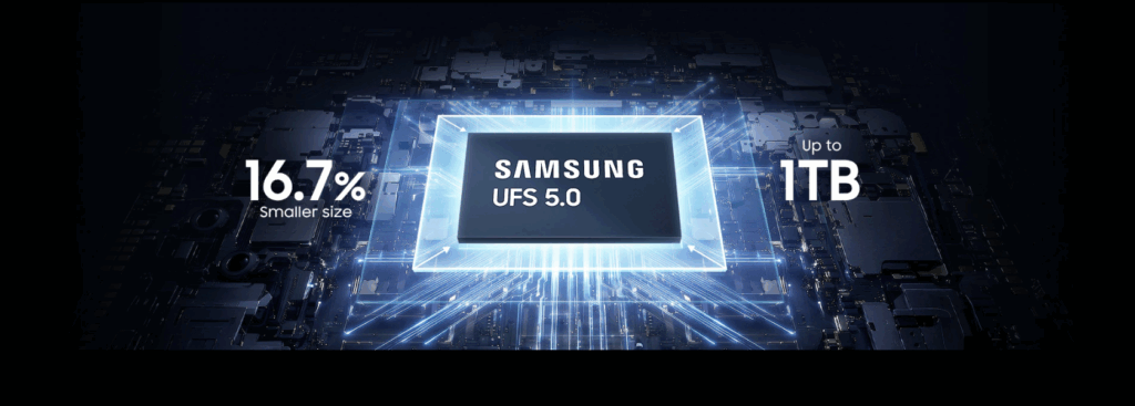
- With capacities up to 1TB on offer, it makes a solid case for displacing existing M.2 drives in laptops, handhelds and game consoles among other hardware
- The chip is also relevant for AI and offers a significant increase in read speeds for AI solutions on the device as a 40% decrease in power consumption compared to UFS 4.1
Samsung has revealed what it says is the industry’s first look at UFS 5.0, a new storage standard for its customers.
The memory and storage giant unveiled its new storage chip on June 23 while positioning its embedded storage standard as a major breakthrough for localized, or on-device, AI solutions.
Samsung claims its chips are based on the standard feature, a sequential read speed of up to 10.8GB/s and a sequential write speed of up to 9.5GB/s, making them more than twice as fast as the previous mainstream UFS standard, which clocked in at 4.2GB/s and 2.8GB/s respectively.
Faster, less power-hungry flash in a more compact package
Samsung’s latest offering isn’t just an iterative upgrade in raw speeds compared to previous generations; it sets the stage for devices yet to come as the world grapples with the need for on-device AI solutions, even as demand for more localized solutions dwarfs expectations among many manufacturers.
With generative AI often leveraging fast NAND flash as a replacement for relatively more expensive DRAM, even as smartphones and computers are increasingly hit by rising prices for both components, Samsung’s UFS 5.0-based offering fills an important gap for many of its OEM customers as well as their own smart devices.
“In the era of on-device AI, storage devices are evolving into a key driver that defines AI experiences,” noted Jangseok Choi, Head of Memory Product Planning at Samsung Electronics.
“As we successfully move beyond the development stage of the industry’s first UFS 5.0 solution, Samsung is setting a new standard for on-the-go storage and will continue to drive innovation for the next-generation mobile platform market.”
As AI solutions range from hyperscalers to things smaller than smartwatches, Samsung’s offering becomes even more important. The package for its solution is 16.7% smaller than its previous generation offering, measuring just 7.5mm x 13mm x 0.9mm, or smaller than most people’s fingernails.
However, Samsung’s main achievement may be the 40% power efficiency it claims to offer compared to its new chip’s predecessor, while delivering speeds that effectively make its solution viable for most local models to run on.
With Samsung touting 5x faster random read speeds, it’s clear that it’s aiming to position its upcoming UFS module as a de facto solution for downstream AI inference, and it could pose a very real threat to some of the most powerful NVMe SSDs out there.
![]()
Follow TechRadar on Google News and add us as a preferred source to get our expert news, reviews and opinions in your feeds.